

Raiden Mark II - Chassis
Note: This is a long one. I’ve been neglecting documenting the project so this post is a catch-up for the last few weeks of work. Future updates will be more frequent and bite-sized. When I think about how to arrange and contain the single-board computers (SBC’s) that make-up the computational part of Raiden Mark II, there are some potentially conflicting requirements: The key areas of improvement over Mark I are
- Smaller
- Quieter
- Lower power consumption
- Less expensive
To this list I also add “repeatable”, because I want to come up with a design that others can use. I don’t want to rely on any unusual, exotic or hard to fabricate components. I also want a design that gives a nod to the computers which inspired it, but not at the cost of the above requirements. After some noodling, sketching and looking at old photographs I settled on an external design inspired by very early personal computers like the Altair 8800, IMSAI 8080, etc.
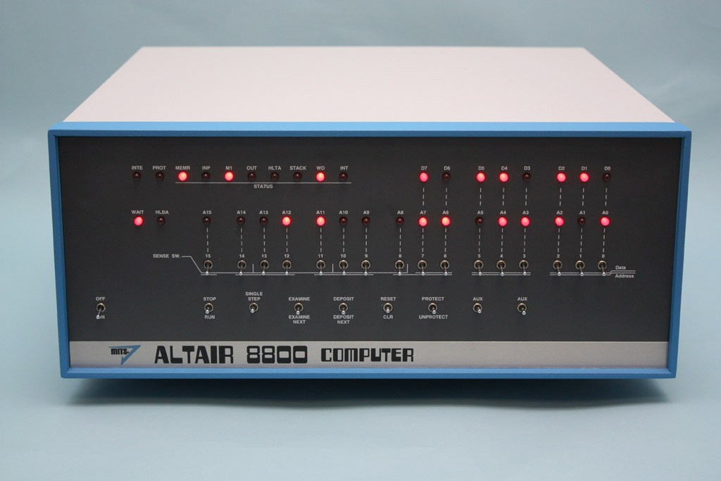 Aside from looking cool, there are some practical aspects to this design. The front panel laden with switches and blinkenlights is used to display status information for each node in the cluster, and the switches are used to control each node individually. These tactile, real-time feedback features are very useful when writing and testing software for a system like this. While the same could be accomplished via software, it’s often faster to be able to glance at an LED to see if there is a problem, or throw a switch to reset a single node. This also removes the need for any kind of video or keyboard connection to each node which is something that was a significant inconvenience when working on Mark I. Another advantage to this design is that the largest part of the chassis (the cabinet) can be found fairly inexpensively on Ebay. This eliminates the need to fabricate large, strong parts and goes a long way toward making it easier to produce more than a one-off build.
  Once I settled on the outside, I had to figure out how to arrange and connect all the components on the inside. I knew I wanted something modular and to minimize the amount of loose wiring. I determined that all the connections I needed to make (aside from network connections) could be found on the 40-pin GPIO header (the “Pi-2 Bus” as it is sometimes called). This being the case I could mount each SBC to a “backplane” using these connectors, similar to how PCI cards work in a regular desktop PC. My first iteration of this was to design a printable backplane which would hold 8 40-pin IDE-style connectors. From these connectors I would run wires to a single connector used to make connections between the backplane and the LED’s, switches, etc. mounted in the front panel. [caption id=“attachment_5023” align=“alignnone” width=“3264”]
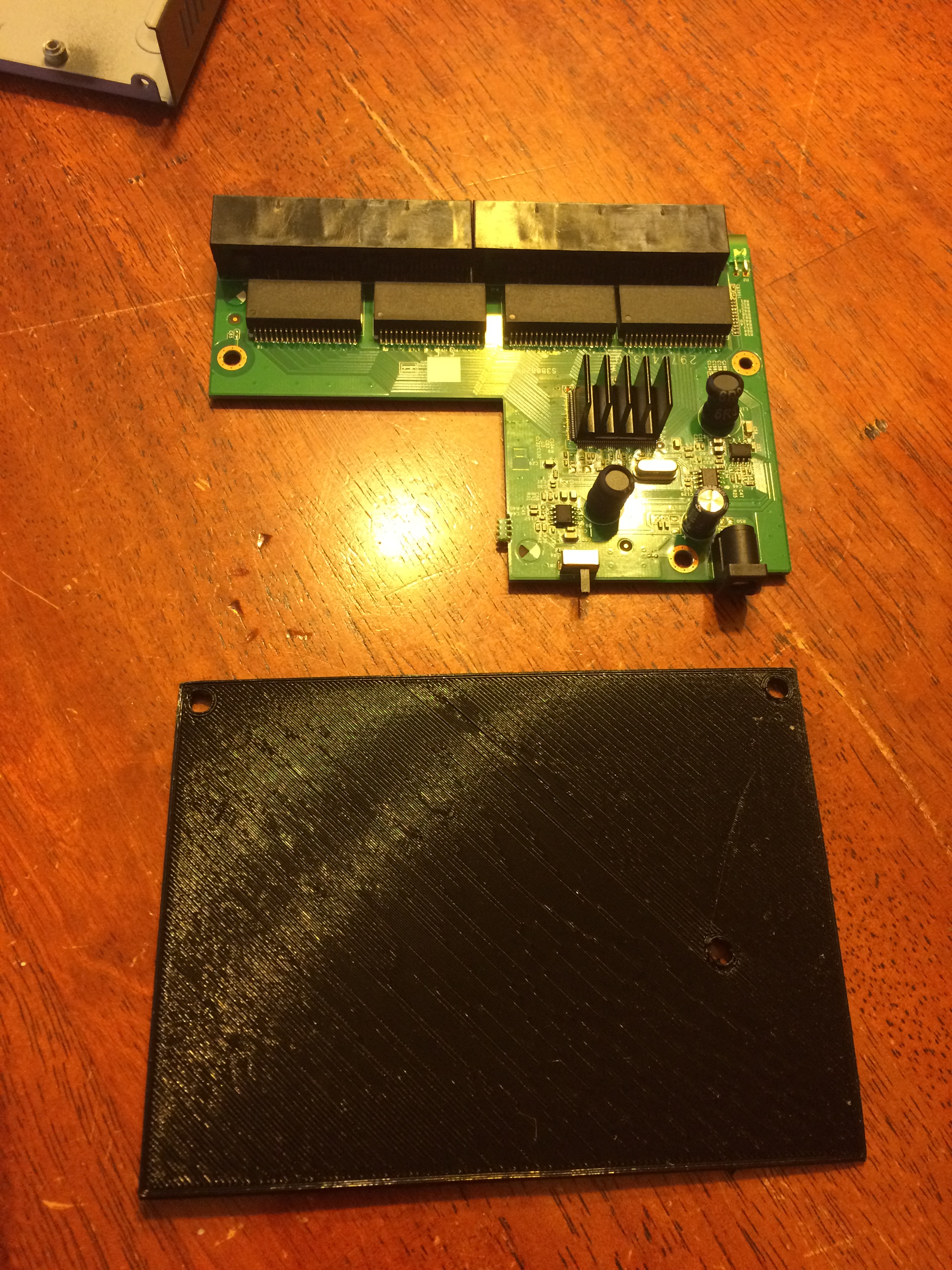 Above: the guts of an 8-port Gigabit Ethernet switch which will be used inside Raiden Mark II. Below: 3D printed “board” to verify size and connecting points for the backplane model.[/caption] This backplane was also designed to align with the mounting holes of the 8-port Ethernet switch I’m including inside the case. The idea was to stack the backplane on top of the switch, that way all of the interconnected pieces could be removed from the chassis as a unit. However, after experimenting with a few different layouts the part became somewhat large and exceeded the size in which my printer is capable of printing reliably. After a few failed attempts at making a printable backplane, I went back to the drawing board.
  My second idea was to use a printed circuit board (pcb) for the backplane. This would not only eliminate the need to print a large part, but it would also allow my to “hide” the wiring between the sbc’s and the front panel connector. This seemed like a great solution, however after looking into several options for creating the boards, I ruled it out due to cost, complexity and lack of flexibility (I’m still at the experimental stage and I don’t know exactly how I want all the connectors wired together yet). In parallel with work on the backplane I was giving thought to the front panel. I knew what I wanted it to look like, but I wasn’t exactly sure how to pull that off. The panel requires many holes for the various indicators and switches and it also requires a number of “legends” as well. I really want to re-create the look of the old machines so the ability to apply these legends to the panel using the right lines and fonts is important, and the sheer number of holes and the accuracy of their locations rules-out my typical approach of grabbing a drill and free-handing it. Also I wanted to come up with a process that could be repeated by others, and might be applicable to some level of volume production. It seemed like using a laser might be the right tool for the job, but the chassis is steel and I know that steel-cutting lasers are not the most accessible tool. So I started thinking about how both tasks might be accomplished using more common 40-50 watt cutting/engraving lasers. [caption id=“attachment_5031” align=“alignnone” width=“828”]
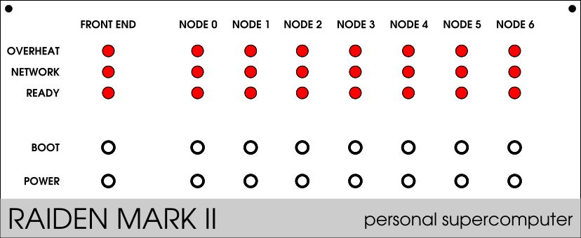 Initial front panel layout (subject to change)[/caption] The first step in this process is to draw the panel using a tool which can output something the laser can consume. I knew Inkscape was capable of this (since I had used it to create drawings for my first CNC project, a really crappy laser engraver ). After a bit of a learning curve I was able to produce a drawing of the panel that came off my laser (printer) while preserving the scale. Aside from scale the hardest part was reliably capturing the dimensions of the hole & attachment points the panel would need.
 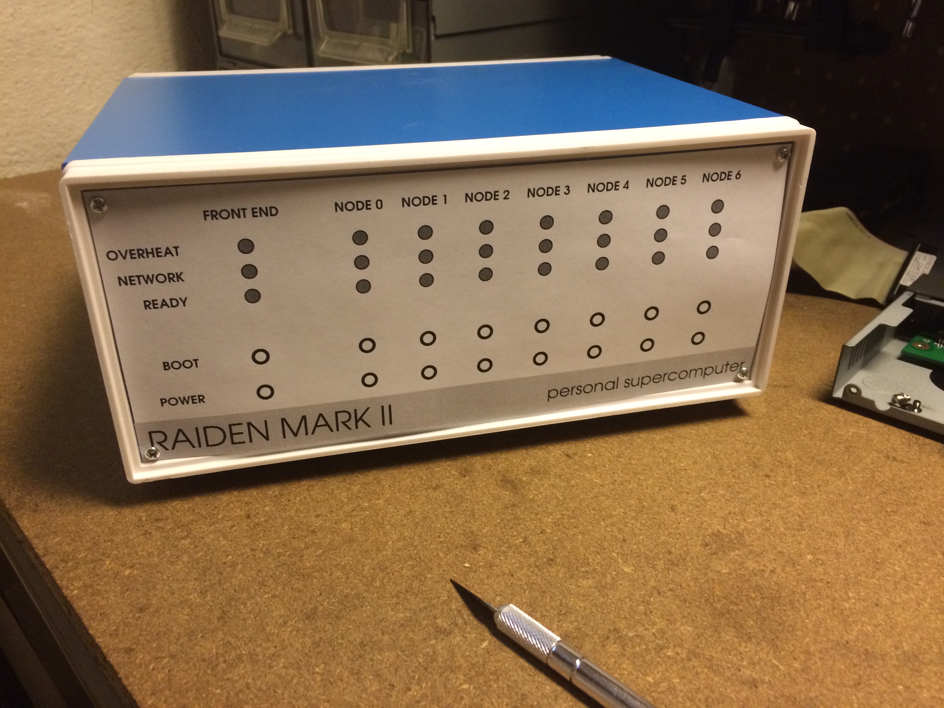 At this point I need to learn more about using a laser and do some experiments to proceed with the panel. I did a lot of reading and decided at some point I want to add a K40 laser to the laboratory, but for now I’m going to setup some time to visit the Idea Studio, learn how to use their laser and run some tests that I’ll elaborate on in a future post. Now that work on the panel is blocked, I switched back to thinking about the backplane. One problem the previous backplane designs don’t address is how the components of the panel are mounted. In the old machines, there was a pcb for the backplane and a second one for the panel, and then holes were cut in the panel where the components mounted on this second board emerged. This means two large pcb’s and a lot of commitment to the connections between parts. Since both of these facts are not ideal for this project (at least at this stage) I started noodling on alternatives to the pcb backplane approach, and came up with something new.